
Photo etching technology does not require expensive DIE's which are also complex shapes with high accuracy of fine precision processing technology that can be manufactured at low cost and quick delivery.
The photoresist pattern is formed on the surface of the metal material such as photography, then dissolved and removed by wet etching the exposed portions of the material mainly in the photoresist, not covered bt the precise shape creation process.
Characteristics of Photo Etching (Cemical miliming) |
|
● |
Pore complex and groove can also easily adjust the depth of groove. |
|
● |
No need for expensive DIE's |
|
● |
Could be applied to most metals for etching technology. |
|
● |
Easy for adjustments that embossing also possible to half the thickness leave. |
|
● |
No alteration process, the characteristics can be obtained as the designer intended. |
|
● |
A prototypr for KFT quick delivery to make measures to organize the special teams. |
|
● |
Two types of image files (DXF/DWG)enabled. |
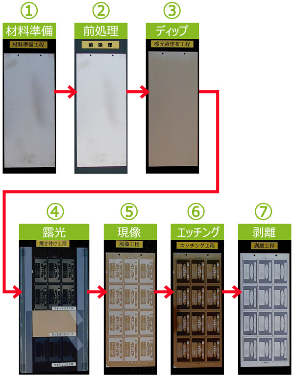
Photo Etching Process |
|
① Material preparetion Cutting for KFT processing handring work size. ② Material cleaning Surface cleaning and proceed chemical pre treatment. ③ Photo resist corting The resist is corted to material surface. ④ Exprosure Setting the part design film that coated material for exprosure. ⑤ Developing Remove the resist of exposed film area. ⑥ Etching Etching material that was developed area on material. ⑦ Remove After etching then remove for remaind corting. |
|
Etching processing progress image |
|
Etching (both side) |
Etching (Half etching) |
||
|
Step 1 |
After Developing
|
After Developing
|
|
|
Step 2 |
Etching (Progress)
|
Etching (Progress)
|
|
|
Step 3 |
Finish Etching
|
Can control Deeps
|


Back to Fact-Link's Top Page