Photo Etching products do not require an expensive DIE cost.
Compare benefits stamping and photo etching.
(A) Shall be required thickness of t=0.3mm or less accurate,especially in.
(B) Point and line size is smaller thickness that need for processing part.
(C) In case of low-volume production the product shall be added to the cost of DIE expenses.
(D) Press part have to create a DIE lead time are longer than etching product lead time (3days).
(E) In case of used material that could cause a change in the properties by the impact of the press.
Approximate specifications of Photo etching.
Plate thickness t=0.10mm - 1.00mm
Material
Stainless steel/Copper/Brass/Steel and special steel (SK/PK)/ special alloy
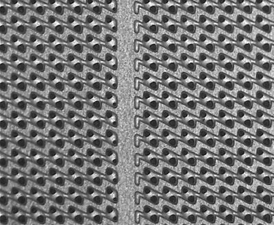
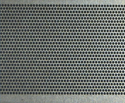
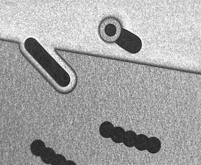
Sample Photo